{domain:"www.qualitydigest.com",server:"169.47.211.87"} Skip to main content

        
User account menu
Main navigation
  • Topics
    • Customer Care
    • Regulated Industries
    • Research & Tech
    • Quality Improvement Tools
    • People Management
    • Metrology
    • Manufacturing
    • Roadshow
    • QMS & Standards
    • Statistical Methods
    • Resource Management
  • Videos/Webinars
    • All videos
    • Product Demos
    • Webinars
  • Advertise
    • Advertise
    • Submit B2B Press Release
    • Write for us
  • Metrology Hub
  • Training
  • Subscribe
  • Log in
Mobile Menu
  • Home
  • Topics
    • Customer Care
    • Regulated Industries
    • Research & Tech
    • Quality Improvement Tools
    • People Management
    • Metrology
    • Manufacturing
    • Roadshow
    • QMS & Standards
    • Statistical Methods
    • Supply Chain
    • Resource Management
  • Login / Subscribe
  • More...
    • All Features
    • All News
    • All Videos
    • Contact
    • Training

New 3D Chips Could Make Electronics Faster, More Energy-Efficient

Low-cost, scalable technology can integrate high-speed gallium nitride transistors onto a standard silicon chip

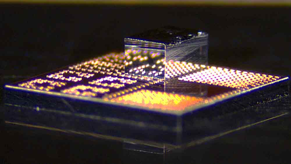
Image courtesy of the researchers

Researchers have developed a new fabrication process that integrates high-performance gallium nitride transistors onto standard silicon CMOS chips in a way that’s low-cost and scalable.

Adam Zewe

MIT

Mon, 07/07/2025 - 12:02
  • Comment
  • RSS

Social Sharing block

  • Print
Body

The advanced semiconductor material gallium nitride (GaN) will likely be key for the next generation of high-speed communication systems and the power electronics needed for state-of-the-art data centers.

ADVERTISEMENT

Unfortunately, the high cost of GaN and the specialization required to incorporate this semiconductor material into conventional electronics have limited its use in commercial applications.

Now, researchers from MIT and elsewhere have developed a new fabrication process that integrates high-performance GaN transistors onto standard silicon CMOS chips in a way that’s low-cost and scalable, as well as compatible with existing semiconductor foundries.

Their method involves building many tiny transistors on the surface of a GaN chip, cutting out each individual transistor, and then bonding just the necessary number of transistors onto a silicon chip using a low-temperature process that preserves the functionality of both materials.

 …

Want to continue?
Log in or create a FREE account.
Enter your username or email address
Enter the password that accompanies your username.
By logging in you agree to receive communication from Quality Digest. Privacy Policy.
Create a FREE account
Forgot My Password
Top Stories
AI May Be Making Your Quality Problem Worse
The 6 Best Quality Management Software Features That Simplify Your QMS
What I Discovered About Quality Concepts by Watching My Newborn Granddaughter
Why Products Still Fail RoHS, REACH, and POPs Compliance
Your AI Model Is Drifting Right Now. Would You Know?

Add new comment

Please login to comment.

© 2026 Quality Digest. Copyright on content held by Quality Digest or by individual authors. Contact Quality Digest for reprint information.
“Quality Digest" is a trademark owned by Quality Circle Institute Inc.

footer
  • Home
  • Print QD: 1995-2008
  • Print QD: 2008-2009
  • Videos
  • Privacy Policy
  • Write for us
footer second menu
  • Subscribe to Quality Digest
  • About Us
  • Contact Us