Image courtesy of the researchers
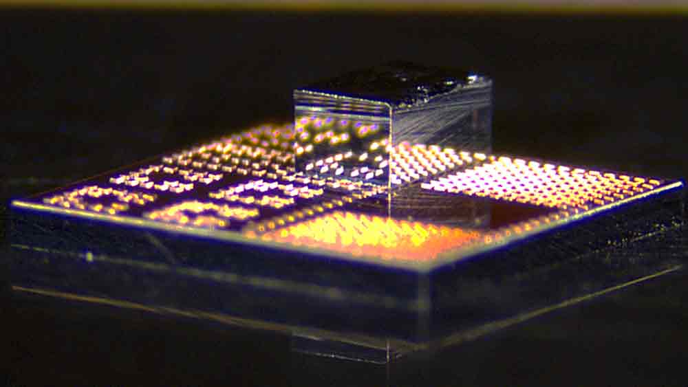
Researchers have developed a new fabrication process that integrates high-performance gallium nitride transistors onto standard silicon CMOS chips in a way that’s low-cost and scalable.
Social Sharing block
The advanced semiconductor material gallium nitride (GaN) will likely be key for the next generation of high-speed communication systems and the power electronics needed for state-of-the-art data centers.
|
ADVERTISEMENT |
Unfortunately, the high cost of GaN and the specialization required to incorporate this semiconductor material into conventional electronics have limited its use in commercial applications.
Now, researchers from MIT and elsewhere have developed a new fabrication process that integrates high-performance GaN transistors onto standard silicon CMOS chips in a way that’s low-cost and scalable, as well as compatible with existing semiconductor foundries.
Their method involves building many tiny transistors on the surface of a GaN chip, cutting out each individual transistor, and then bonding just the necessary number of transistors onto a silicon chip using a low-temperature process that preserves the functionality of both materials.
…
Add new comment