{domain:"www.qualitydigest.com",server:"169.47.211.87"} Skip to main content

User account menu
Main navigation
  • Topics
    • Customer Care
    • FDA Compliance
    • Healthcare
    • Innovation
    • Lean
    • Management
    • Metrology
    • Operations
    • Risk Management
    • Six Sigma
    • Standards
    • Statistics
    • Supply Chain
    • Sustainability
    • Training
  • Videos/Webinars
    • All videos
    • Product Demos
    • Webinars
  • Advertise
    • Advertise
    • Submit B2B Press Release
    • Write for us
  • Metrology Hub
  • Training
  • Subscribe
  • Log in
Mobile Menu
  • Home
  • Topics
    • 3D Metrology-CMSC
    • Customer Care
    • FDA Compliance
    • Healthcare
    • Innovation
    • Lean
    • Management
    • Metrology
    • Operations
    • Risk Management
    • Six Sigma
    • Standards
    • Statistics
    • Supply Chain
    • Sustainability
    • Training
  • Login / Subscribe
  • More...
    • All Features
    • All News
    • All Videos
    • Contact
    • Training

Bede X-ray Metrology Partners with Belgian Research Center

Quality Digest
Wed, 09/13/2006 - 22:00
  • Comment
  • RSS

Social Sharing block

  • Print
Body

Bede X-ray Metrology, a provider of X-ray metrology solutions to the semiconductor industry, has announced a collaboration with IMEC, a Belgian nanoelectronics and nanotechnology research center.

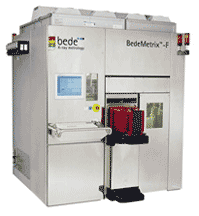
The companies will investigate the use of X-ray metrology in the process control of new semiconductor materials used at the 45 nm technology node and below, using Bede’s BedeMetrix-L and Microsource with ScribeView optics X-ray system. The BedeMetrix-L uses a combination of high-resolution X-ray diffraction, X-ray diffraction and X-ray reflectivity techniques on a single platform for a wide range of front- and back-end process control applications.

X-ray metrology is an important technology for controlling semiconductor processes as the technology nodes shrink, especially at 45 nm and below.

“Bede X-ray Metrology will be used for the measurement of critical process control parameters needed in the use of advanced semiconductor materials for device fabrication,” says Luc Van den hove, IMEC silicon process and device technology vice president. “We are pleased that our research will benefit from Bede’s expertise in X-ray-based process metrology.”

 …

Want to continue?
Log in or create a FREE account.
Enter your username or email address
Enter the password that accompanies your username.
By logging in you agree to receive communication from Quality Digest. Privacy Policy.
Create a FREE account
Forgot My Password

Add new comment

Image CAPTCHA
Enter the characters shown in the image.
Please login to comment.
      

© 2025 Quality Digest. Copyright on content held by Quality Digest or by individual authors. Contact Quality Digest for reprint information.
“Quality Digest" is a trademark owned by Quality Circle Institute Inc.

footer
  • Home
  • Print QD: 1995-2008
  • Print QD: 2008-2009
  • Videos
  • Privacy Policy
  • Write for us
footer second menu
  • Subscribe to Quality Digest
  • About Us
  • Contact Us