Featured Product
This Week in Quality Digest Live
Metrology Features
Harish Jose
Using OC curves to generate reliability/confidence values
Scott Knoche
Choosing the best, most appropriate add-ons makes your work faster and easier
Adam Zewe
Key component for portable mass spectrometers
Peter Büscher
Identify contaminated areas and take steps to optimize them
Silke von Gemmingen
New approach investigates damage due to environmental fluctuation on textile artifacts

More Features

Metrology News
Improving quality control of PCBAs and optimizing X-ray inspection
10-year technology partnership includes sponsorship of quality control lab
MM series features improved functionality and usability
Features improved accuracy, resolution, versatility, and efficiency
Versatile CT solution for a range of 3D metrology, research, and evaluation applications
Adding its new SV series to NASCAR’s all-time leader in wins
Precise, high-speed inspection system makes automotive component production go faster
Upgrade to Mitutoyo’s latest CMM, vision, or form-measuring equipment
International Paper Co. saves money with Radian Plus laser tracker and vProbe

More News

NIST

Metrology

Tracking Nanoparticles in 3-D

Published: Wednesday, April 9, 2008 - 22:00

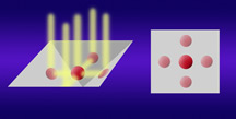
Heart of the orthogonal tracking microscope system developed at NIST is this nanoparticle solution sample well etched in silicon. Careful orientation of the silicon crystal makes it possible to chemically etch angled sides in the well so smooth they act as mirrors. In this configuration, four side views of a nanoparticle floating in solution (left) are reflected up. A microscope above the well sees the real particle (center, right) and four reflections that show the particle’s vertical position.


(NIST: Gaithersburg, Maryland) -- A clever new microscope design allows nanotechnology researchers at the National Institute of Standards and Technology to track the motions of nanoparticles in solution as they dart around in three dimensions. The researchers hope that the technology, which NIST plans to patent, will lead to a better understanding of the dynamics of nanoparticles in fluids and, ultimately, process control techniques to optimize the assembly of nanotech devices.

While some nanoscale fabrication techniques borrow from the lithography and solid state methods of the microelectronics industry, an equally promising approach relies on “directed self-assembly.” This capitalizes on physical properties and chemical affinities of nanoparticles in solutions to induce them to gather and arrange themselves in desired structures at desired locations. Potential products include extraordinarily sensitive chemical and biological sensor arrays, and new medical and diagnostic materials based on “quantum dots” and other nanoscale materials. But when your product is too small to be seen, monitoring the assembly process is difficult.

Microscopes can help, but a microscope sees a three-dimensional fluid volume as a 2-D plane. There’s no real sense of the up-and-down movement of particles in its field of view except that they get more or less fuzzy as they move across the plane where the instrument is in focus. To date, attempts to provide a 3-D view of the movements of nanoparticles in solution largely have relied on that fuzziness. Optics theory and mathematics can estimate how far a particle is above or below the focal plane based on diffraction patterns in the fuzziness. The math, however, is extremely difficult and time-consuming and the algorithms are imprecise in practice.

One alternative, NIST researchers reported at the annual March meeting of the American Physical Society, is to use geometry instead of algebra. Specifically, angled side walls of the microscopic sample well can be used to act as mirrors to reflect side views of the volume up to the microscope at the same time as the top view (The typical sample well is 20 microns square and 15 microns deep.) The microscope sees each particle twice, one image in the horizontal plane and one in the vertical. Because the two planes have one dimension in common, it’s a simple calculation to correlate the two and figure out each particle’s 3-D path. “Basically, we reduce the problem of tracking in 3-D to the problem of tracking in 2-D twice,” explains lead author Matthew McMahon.

The 2-D problem is simpler to solve—several software techniques can calculate and track 2-D position to better than 10 nanometers. Measuring the nanoparticle motion at that fine scale—speeds, diffusion, and the like—will allow researchers to calculate the forces acting on the particles and better understand the basic rules of interaction between the various components. That in turn will allow better design and control of nanoparticle assembly processes.

For more information, visit www.nist.gov/public_affairs/techbeat/tb2008_0318.htm#ortho

Discuss

About The Author

NIST’s picture

NIST

Founded in 1901, the National Institute of Standards and Technology (NIST) is a nonregulatory federal agency within the U.S. Department of Commerce. Headquartered in Gaithersburg, Maryland, NIST’s mission is to promote U.S. innovation and industrial competitiveness by advancing measurement science, standards, and technology in ways that enhance economic security and improve our quality of life.