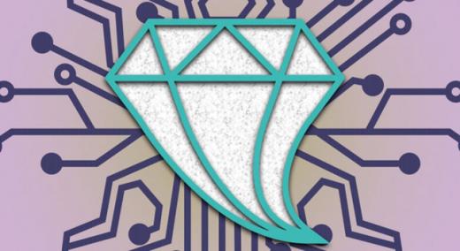
Introducing a small amount of strain into crystalline materials, such as diamond or silicon, can produce significant changes in their properties, researchers have found. The mechanical strain is represented here as a deformation in the diamond's shape. Image: Chelsea Turner, MIT
Applying just a bit of strain to a piece of semiconductor or other crystalline material can deform the orderly arrangement of atoms in its structure enough to cause dramatic changes in its properties, such as the way it conducts electricity, transmits light, or conducts heat.
|
ADVERTISEMENT |
Now, a team of researchers at MIT and in Russia and Singapore have found ways to use artificial intelligence to help predict and control these changes, potentially opening up new avenues of research on advanced materials for future high-tech devices.
The findings appear this month in the Proceedings of the National Academy of Sciences, in a paper authored by Ju Li, MIT professor of nuclear science and engineering and of materials science and engineering; MIT Principal Research Scientist Ming Dao, and MIT graduate student Zhe Shi, with Evgeni Tsymbalov and Alexander Shapeev at the Skolkovo Institute of Science and Technology in Russia; and Subra Suresh, the Vannevar Bush Professor Emeritus and former dean of engineering at MIT and current president of Nanyang Technological University in Singapore.
…

Add new comment