{domain:"www.qualitydigest.com",server:"169.47.211.87"} Skip to main content

User account menu
Main navigation
  • Topics
    • Customer Care
    • FDA Compliance
    • Healthcare
    • Innovation
    • Lean
    • Management
    • Metrology
    • Operations
    • Risk Management
    • Six Sigma
    • Standards
    • Statistics
    • Supply Chain
    • Sustainability
    • Training
  • Videos/Webinars
    • All videos
    • Product Demos
    • Webinars
  • Advertise
    • Advertise
    • Submit B2B Press Release
    • Write for us
  • Metrology Hub
  • Training
  • Subscribe
  • Log in
Mobile Menu
  • Home
  • Topics
    • 3D Metrology-CMSC
    • Customer Care
    • FDA Compliance
    • Healthcare
    • Innovation
    • Lean
    • Management
    • Metrology
    • Operations
    • Risk Management
    • Six Sigma
    • Standards
    • Statistics
    • Supply Chain
    • Sustainability
    • Training
  • Login / Subscribe
  • More...
    • All Features
    • All News
    • All Videos
    • Contact
    • Training

New Computer Vision Method Helps Speed Electronic Materials Screening

Technique characterizes a material’s electronic properties 85 times faster than conventional methods

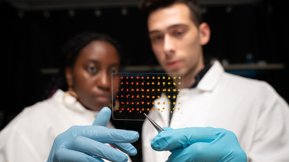
MIT graduate students Eunice Aissi (left) and Alexander Siemenn have developed a technique that automatically analyzes visual features in printed samples (pictured) to quickly determine key properties of new and promising semiconducting materials. Photo: Bryce Vickmark

Jennifer Chu
Wed, 06/26/2024 - 12:03
  • Comment
  • RSS

Social Sharing block

  • Print
Body

Boosting the performance of solar cells, transistors, LEDs, and batteries will require better electronic materials made from novel compositions that have yet to be discovered.

ADVERTISEMENT

To speed up the search for advanced functional materials, scientists are using AI tools to identify promising materials from hundreds of millions of chemical formulations. In tandem, engineers are building machines that can print hundreds of material samples at a time based on chemical compositions tagged by AI search algorithms.

But to date, there’s been no similarly speedy way to confirm that these printed materials actually perform as expected. This last step of material characterization has been a major bottleneck in the pipeline of advanced materials screening.

Now, a new computer vision technique developed by MIT engineers significantly speeds up the characterization of newly synthesized electronic materials. The technique automatically analyzes images of printed semiconducting samples and quickly estimates two key electronic properties for each sample: band gap (a measure of electron activation energy) and stability (a measure of longevity).

 …

Want to continue?
Log in or create a FREE account.
Enter your username or email address
Enter the password that accompanies your username.
By logging in you agree to receive communication from Quality Digest. Privacy Policy.
Create a FREE account
Forgot My Password

Add new comment

Image CAPTCHA
Enter the characters shown in the image.
Please login to comment.
      

© 2025 Quality Digest. Copyright on content held by Quality Digest or by individual authors. Contact Quality Digest for reprint information.
“Quality Digest" is a trademark owned by Quality Circle Institute Inc.

footer
  • Home
  • Print QD: 1995-2008
  • Print QD: 2008-2009
  • Videos
  • Privacy Policy
  • Write for us
footer second menu
  • Subscribe to Quality Digest
  • About Us
  • Contact Us