{domain:"www.qualitydigest.com",server:"169.47.211.87"} Skip to main content

User account menu
Main navigation
  • Topics
    • Customer Care
    • FDA Compliance
    • Healthcare
    • Innovation
    • Lean
    • Management
    • Metrology
    • Operations
    • Risk Management
    • Six Sigma
    • Standards
    • Statistics
    • Supply Chain
    • Sustainability
    • Training
  • Videos/Webinars
    • All videos
    • Product Demos
    • Webinars
  • Advertise
    • Advertise
    • Submit B2B Press Release
    • Write for us
  • Metrology Hub
  • Training
  • Subscribe
  • Log in
Mobile Menu
  • Home
  • Topics
    • 3D Metrology-CMSC
    • Customer Care
    • FDA Compliance
    • Healthcare
    • Innovation
    • Lean
    • Management
    • Metrology
    • Operations
    • Risk Management
    • Six Sigma
    • Standards
    • Statistics
    • Supply Chain
    • Sustainability
    • Training
  • Login / Subscribe
  • More...
    • All Features
    • All News
    • All Videos
    • Contact
    • Training

MIT Engineers Grow ‘High-Rise’ 3D Chips

An electronic stacking technique could exponentially increase the number of transistors on chips

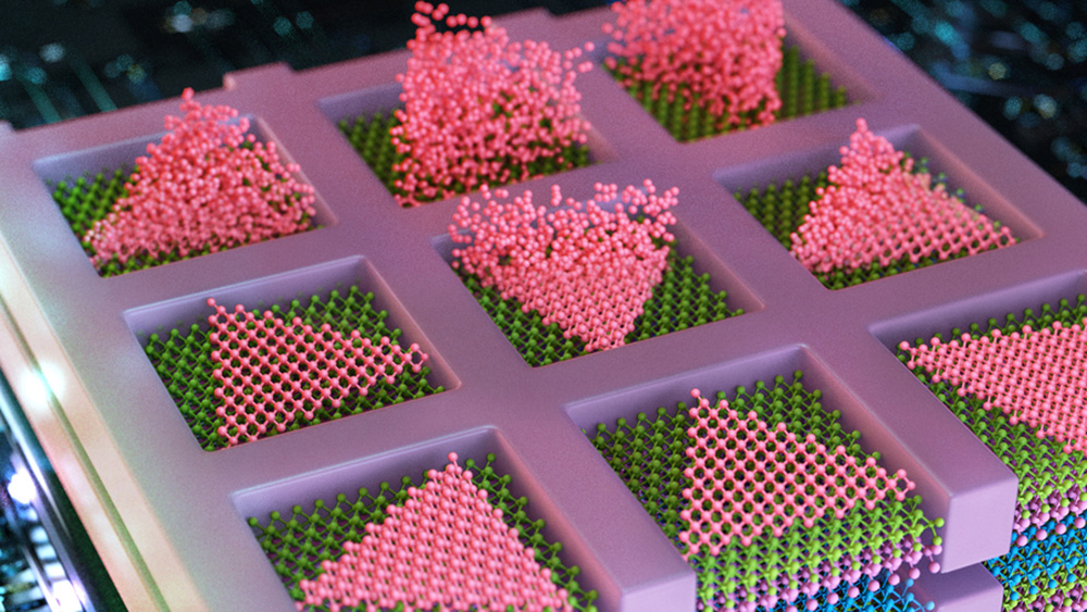
MIT engineers have developed a method to seamlessly stack electronic layers to create faster, denser, more powerful computer chips. The team deposits semiconducting particles (in pink) as triangles within confined squares, creating high-quality electronic elements directly atop other semiconducting layers (shown in layers of purple, blue, and green). Credit: Cube 3D Graphic

Jennifer Chu
Thu, 01/16/2025 - 12:02
  • Comment
  • RSS

Social Sharing block

  • Print
Body

The electronics industry is approaching a limit to the number of transistors that can be packed onto the surface of a computer chip. So chip manufacturers are looking to build up, rather than out.

ADVERTISEMENT

Instead of squeezing ever-smaller transistors onto a single surface, the industry is aiming to stack multiple surfaces of transistors and semiconducting elements—akin to turning a ranch house into a high-rise. Such multilayered chips could handle exponentially more data and carry out many more complex functions than today’s electronics.

A significant hurdle, however, is the platform on which chips are built. Today, bulky silicon wafers serve as the main scaffold on which high-quality, single-crystalline semiconducting elements are grown. Any stackable chip would have to include thick silicon “flooring” as part of each layer, slowing down any communication between functional semiconducting layers.

Now, MIT engineers have found a way around this hurdle with a multilayered chip design that doesn’t require any silicon wafer substrates and works at temperatures low enough to preserve the underlying layer’s circuitry.

 …

Want to continue?
Log in or create a FREE account.
Enter your username or email address
Enter the password that accompanies your username.
By logging in you agree to receive communication from Quality Digest. Privacy Policy.
Create a FREE account
Forgot My Password

Add new comment

Image CAPTCHA
Enter the characters shown in the image.
Please login to comment.
      

© 2025 Quality Digest. Copyright on content held by Quality Digest or by individual authors. Contact Quality Digest for reprint information.
“Quality Digest" is a trademark owned by Quality Circle Institute Inc.

footer
  • Home
  • Print QD: 1995-2008
  • Print QD: 2008-2009
  • Videos
  • Privacy Policy
  • Write for us
footer second menu
  • Subscribe to Quality Digest
  • About Us
  • Contact Us