{domain:"www.qualitydigest.com",server:"169.47.211.87"} Skip to main content

User account menu
Main navigation
  • Topics
    • Customer Care
    • FDA Compliance
    • Healthcare
    • Innovation
    • Lean
    • Management
    • Metrology
    • Operations
    • Risk Management
    • Six Sigma
    • Standards
    • Statistics
    • Supply Chain
    • Sustainability
    • Training
  • Videos/Webinars
    • All videos
    • Product Demos
    • Webinars
  • Advertise
    • Advertise
    • Submit B2B Press Release
    • Write for us
  • Metrology Hub
  • Training
  • Subscribe
  • Log in
Mobile Menu
  • Home
  • Topics
    • 3D Metrology-CMSC
    • Customer Care
    • FDA Compliance
    • Healthcare
    • Innovation
    • Lean
    • Management
    • Metrology
    • Operations
    • Risk Management
    • Six Sigma
    • Standards
    • Statistics
    • Supply Chain
    • Sustainability
    • Training
  • Login / Subscribe
  • More...
    • All Features
    • All News
    • All Videos
    • Contact
    • Training

Engineers Mix and Match Materials to Make New Stretchy Electronics

Next-generation devices made with new “peel and stack” method may include electronic chips worn on the skin

Jennifer Chu
Wed, 02/26/2020 - 12:01
  • Comment
  • RSS

Social Sharing block

  • Print
Body

First published Feb. 5, 2020, on MIT News.

At the heart of any electronic device is a cold, hard computer chip, covered in a miniature city of transistors and other semiconducting elements. Because computer chips are rigid, the electronic devices that they power, such as our smartphones, laptops, watches, and televisions, are similarly inflexible.

Now a process developed by MIT engineers may be the key to manufacturing flexible electronics with multiple functionalities in a cost-effective way.

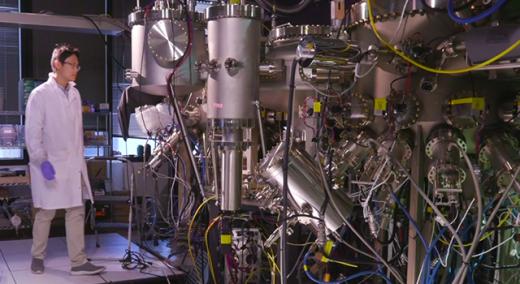
The process is called  “remote epitaxy” and involves growing thin films of semiconducting material on a large, thick wafer of the same material, which is covered in an intermediate layer of graphene. Once the researchers grow a semiconducting film, they can peel it away from the graphene-covered wafer and then reuse the wafer, which itself can be expensive depending on the type of material it’s made from. In this way, the team can copy and peel away any number of thin, flexible semiconducting films, using the same underlying wafer.

 …
Want to continue?
Log in or create a FREE account.
Enter your username or email address
Enter the password that accompanies your username.
By logging in you agree to receive communication from Quality Digest. Privacy Policy.
Create a FREE account
Forgot My Password

Add new comment

Image CAPTCHA
Enter the characters shown in the image.
Please login to comment.
      

© 2025 Quality Digest. Copyright on content held by Quality Digest or by individual authors. Contact Quality Digest for reprint information.
“Quality Digest" is a trademark owned by Quality Circle Institute Inc.

footer
  • Home
  • Print QD: 1995-2008
  • Print QD: 2008-2009
  • Videos
  • Privacy Policy
  • Write for us
footer second menu
  • Subscribe to Quality Digest
  • About Us
  • Contact Us