by Shane Woody, Ph.D.
During the past decade, a number of innovative manufacturing processes--such as laser drilling, micromilling, and advanced electrical discharge machining (EDM) automation--have produced remarkable microscale components at economical production rates. These components are now integrated into many of our everyday consumer products that span a wide range of industries. However, inspecting these features isn’t always simple, especially when they have a narrow or deep features on the component. Moreover, new nanotechnology applications will soon hit the marketplace, and tools for both metrology and manufacturing will be critical to integrating nanotechnology with micro and mesoscale technologies.
The report, “Instrumentation and Metrology for Nanotechnology,” presented at the National Nanotechnology Initiative Workshop in January 2004, and the report “An Assessment of the United States Measurement System: Addressing Measurement Barriers to Accelerated Innovation,” appearing in the National Institute of Standards and Technology’s Special Publication 1048 in February 2007 (online at http://usms.nist.gov ) have both identified metrology tools as bottlenecks to innovation. Asia and Europe, for example, are sharply and competitively focused on manufacturing and metrology for microscale and nanoscale industries. Manufacturers in the United States have also realized that shifting their focus from macro to nanoscale will be critical for sustaining a competitive advantage in the global economy. Being able to manufacture microscale and nanoscale features will speed technological progress but will also create challenges in fabrication and process metrology. NIST, a nonregulatory federal agency within the U.S. Department of Commerce, has set a goal to “develop and characterize advanced probing technologies to bring microfeature (100 µm–500 µm) measurement capacity to a level suitable for NIST SP-250 calibrations.” (View online at http://usms.nist.gov.) The development of metrology tools that can function at these scales will continue to be a pressing need to enable scientific insight for emerging markets, predictive process capabilities, enhanced functionality, and connectivity across scales.
In nature, on a microscale level, we observe feature sizes to be substantially different in proportions compared with the macroscale world, specifically when comparing the ratio between the feature width and length, i.e., the aspect ratio. Consider, for example, the legs of elephants compared to the legs of ants. An ant is less influenced by gravitational forces, and so the aspect ratio of its leg width to length is substantially higher, providing more mechanical levering ability. Designers have learned from nature, and many microscale components mimic nature in that they have high aspect ratios (e.g., greater than 40:1) to obtain peak performance benefits. Such high aspect-ratio features present unique challenges for achieving dimensional measurements.
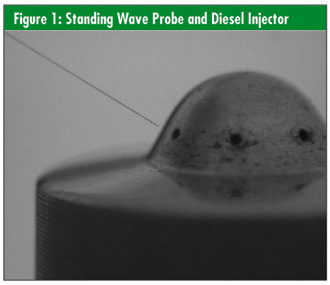
In her paper, “The Need for Metrology in Nanotechnology,” compiled for the High Level Expert Group on Measurement and Testing at the Danish Institute of Fundamental Metrology, Kim Carneiro writes, “Any activity within science and technology must be accompanied by reference measurements (i.e., metrology tools) to ensure that quantitative results are comparable and products interchangeable.” Scientists need metrology tools capable of measuring deep micro and nanoscale cavities and features. Take, for example, a common yet critical component in diesel automobile engines, the diesel injector. A diesel injector spray hole is approximately 100 µm in diameter. Future generations of this component will approach 50-µm diameters with depths exceeding 2 mm, as seen in figure 1 at right. Injector designs use a high aspect ratio to help atomize the fuel in the chamber and control the combustion process. The size and shape of the hole along this 2-mm length directly affects functionality, and therefore the engine’s efficiency and emissions.
One of the major manufacturing challenges is to measure the geometry of these holes so that computer models may be validated and manufacturing processes enhanced. This capability will affect the design of new injectors and lead to increased efficiency and lower emissions. Federal laws dictate that, by next year, off-road diesel engines must lessen particulate output by 95 percent and NO 2 by 90 percent. “Regulating Air Pollution from Diesel Trucks: A Model Rule for States,” a July 2001 report issued by the State and Territorial Air Pollution Program Administration (STAPPA) and the Association of Local Air Pollution Control Officials (ALAPCO), estimated that reducing emissions could prevent 8,500 premature deaths in the United States per year and save up to $67 billion annually. (View online at www.4cleanair.org/DieselTrucks.pdf.) This is one of many compelling examples in micromanufacturing that will affect our social and economic well-being.
Achieving this capability will require “the development of novel probes that are capable of measuring the tiny features that are encountered in the field of microsystems,” according to the United Kingdom’s National Measurement Laboratory, in its report “Nano Dimensional Metrology.” In terms of metrology, the difficulty is that the measurement sensor should be at least ten times smaller than the measured feature (i.e., the size of the hole) to adequately measure the feature’s form and the asperities residing on it. Taking this into account, a tactile probe would need to measure less than 5 µm in diameter with a length of up to 2 mm to allow deep measurements into the feature. That’s a 400:1 aspect ratio.
The lack of metrology tools that operate across multiple dimensional scales and therefore provide traceable measurements is a primary barrier to fully realizing many applications at these engineering scales. Essentially, the inability to measure challenging features leads to an inability to improve and understand process behaviors. Many emerging nano and micromanufacturing systems must integrate functionality across multiple dimensional scales (e.g., biomicroelectromechanical systems and micro or nanofluidics). The complexity of these systems requires each layer to be designed and integrated seamlessly. Traditional coordinate measuring machines (CMM) accommodate larger workpieces on the order of millimeters, with position and measurement capabilities at or near 1 µm. Many technologies developed for the smaller features and higher resolutions used in microscale inspection--such as scanning probe microscopy (SPM)--are considered 2.5-D measurement devices. That is, they’re limited in their capability when attempting to measure high aspect-ratio features. As a result, true 3-D metrology is nonexistent in both nanoscale and microscale when considering high aspect-ratio measurements.
Historically, CMMs are used for dimensional metrology and are one of the few traceable methods that can provide true 3-D measurement capability. State-of-the-art CMM techniques for microscale component geometry usually employ touch triggering (i.e., intermittent contact) or scanning as the contact interaction-based measurement technique. Customer requirements for measuring small or fragile parts are pushing traditional touch-probe equipment to the limit. However, until a technology emerges that replaces touch probes for accurate measurement in hard-to-reach places, look for touch-probe technology to continue evolving toward smaller and smaller probes. A handful of commercially available CMMs have a microprobe integrated into the system, as do several specialty systems at government laboratories (such as the Moore M48 at NIST), and any number of university- built metrology platforms. Although these machines are good, and in many cases excellent, metrology platforms with nanometric scales, their primary limitation is the lack of a reliable, robust, capable micro and/or nanoprobe.
The current state of the art for microprobes is to mimic the probing technology from macroscale CMMs, where a 3-D measuring machine employs a sensor probe with a spherical ball attached to the end of a stylus. This creates a geometrically defined solid contact that protrudes beyond the shank. However, many small 3-D structures require probe-tip contact diameters of only a few micrometers in size to resolve small spatial features. It’s challenging if not close to impossible to scale down this technology to make it functional at the micro and nanometer scales. For example, current optical technologies can’t be scaled small enough to measure into deep, narrow features, and optical resolution is limited by the wavelength of light. X-ray imaging provides a picture of the feature but lacks traceable metrology information. Functional testing is costly and may not provide sufficient information about engineers’ models or the manufacturing process. Therefore, the bottleneck to realizing true 3-D metrology on a microscale and nanoscale level lies mostly with the sensor.
Most microscale sensing technologies are still fraught with problems such as probe susceptibility to environmental conditions--e.g., humidity and surface interactions such as stiction. In contact microscale probing, adhesion and other contact interactions between the workpiece and probe tip at the nanometer and micrometer feature level are significant. This is especially true for high aspect-ratio fiber sensors where the entire stylus is compliant and low in mechanical stiffness. As a result, the sensor tip snaps into contact with the surface and continues to remain attracted or “stuck” to the surface, even when severely bent while it’s pulled away from the surface. This adhesion problem may be due to any number of problems related to meniscus forces (i.e., thin water layers building on the workpiece surface), electrostatic forces, or weaker attraction forces such as Van der Waals dispersion forces.
This example shows the types of problems we face in the quality community when we consider using high aspect-ratio sensors. The problem is multifaceted and includes attraction force effects, dirt or debris collecting on the sensor, and influences from turbulent airflow. In the case of attraction-force problems, these adhesion forces reduce the accuracy and repeatability of microscale scanning probes. Correspondingly, at these scales, the related frictional forces introduce uncertainties due to structural distortions caused by the interaction between the probe tip and workpiece surfaces. Moreover, contact forces of many of these touch probes are often greater than one µN and for small probe tip radii can elastically or even plastically deform the measured surface.
During the past three years, InsituTec Inc., a provider of ultra-precision measurement solutions, has partnered with the Center for Precision Metrology at the University of North Carolina to focus efforts in innovative microscale sensors for dimensional metrology. From this work, a novel tactile sensing method has emerged known as a standing wave sensor. This is a new class of sensor utilizing ultrasonic frequencies to shape a pronounced tip on the end of a microscale fiber. Several globally recognized metrology companies commercially produce vibrating tactile probes. However, the standing wave sensor is unique because the tool purposely creates or shapes a pronounced tip on the end of the sensor by employing ultrasonic frequencies. Ultrasonic is typically classified as producing drive frequencies from 20,000 to 3 million times per second. In the case of the standing wave sensor, the fiber is vibrated back and forth 32,000 times per second using a crystal oscillating tuning fork. A time-averaged picture of the oscillating fiber will produce an image of the oscillating probe as a solid volume, traced out by the path of the fiber’s outer surface, which will have a defined geometrical pattern on the end, as seen in figure 2 at right. The actual probe is composed only of the fiber; however, the virtual tip is composed of an integral of the path produced by the tip. Furthermore, the outer locus of the virtual tip is composed of the total sum of motion produced by the very end of the fiber, thereby generating a pseudo-field capable of interacting with other solids and surfaces in near proximity. This programmable field (or virtual tip) may be strategically employed in both microscale and nanoscale metrology.
The sensor uses resonant frequencies to generate the standing wave as well as phase-sensitive electronics to detect interactions between the tip and workpiece. First, the tuning fork provides both an input and output response. In practice, a drive signal is transferred to the tuning fork resonator to drive the first mode-resonant frequency. The output response of the tuning fork is monitored. Once the fiber’s virtual tip is contacted against a specimen, the output signal from the tuning fork will change in both amplitude and phase. These signal characteristics are then signal-conditioned and used as the tactile probe’s contact signal. For example, the sensors can be attached to custom metrology motion-control devices capable of positioning to 1 nm. In a touch triggering mode, the sensor has demonstrated 10-nm repeatability. The sensor is currently being used in scanning mode as well. In this configuration, the sensor is locked at a constant force of less than 1 µN and then scanned continuously along the surface using the same constant force. This approach enables approximately 100 to 1,000 data points per second to be extracted from the measurement process.
The virtual tip is shaped at the end of a 4 mm-long fiber that has a cross-section of 7.5 µm, a 500:1 aspect ratio. The tip shaped at the end of this aspect-ratio sensor will swing further out than anywhere e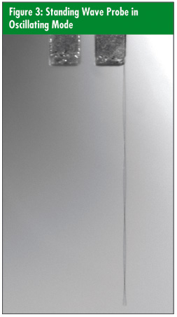 lse along the shaft. As a result, the tactile sensor can be inserted into what previously seemed to be impossible-to-measure features, such as small microscale holes. lse along the shaft. As a result, the tactile sensor can be inserted into what previously seemed to be impossible-to-measure features, such as small microscale holes.
In the world of microscale sensing, conventional sensors inevitably will stick to the surfaces because of the attraction forces mentioned earlier. These forces are a distinct problem because the sensors will produce false readings and are limited to touch triggering. This is because the sensors must be small in diameter but still long and slender. The standing wave sensor overcomes attraction force effects because the oscillating shank stores enough energy in the vibrating tip to overcome adhesive interactions. Overcoming these attraction forces enables higher- precision measurements as well as the ability to continuously scan surfaces. Additionally, the high aspect-ratio fibers provide minimal damage during collisions.
Because of the fiber’s small diameter and long length, the fibers are compliant in the lateral direction (often the direction in which collision occurs). We observed that if the probes are severely bent, they return to their original shape once released, proving to be very robust. Additionally, the sensor with an accompanying metrology platform has demonstrated the ability to overcome attraction forces when the standing wave is active. We have completed step height measurements with 10-nm repeatability and measured holes less than 120 µm in diameter while using the probe in a continuous scanning mode.
Continuing research is focused on multidimensional sensing capability and scaling the methodology for nanoscale science. Virtual tip shaping is expected to provide significant improvements in quality inspection on a microscale and nanoscale level.
Shane Woody, Ph.D., is co-founder of InsituTec Inc., a company dedicated to in-process inspection equipment. He’s worked in research and development of metrology tools for 12 years, specializing in gauging and sensing. For more information, visit www.insitutec.com.
|

 Metrology for micro and nanoscale
 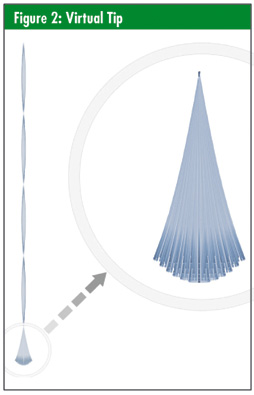 Standing wave sensors