| by Ralph Leseberg
Many of the electronic products we use rely on advances in semiconductor manufacturing. Today’s
most demanding high-technology manufacturing operations for the heads in disk drives, micro-electro-mechanical systems (MEMS), micro-optical-electro-mechanical system (MOEMS) devices, and other semiconductor devices require dimensional or positioning accuracies in the submicron to nanometer range (10-6 to 10-9 m). Those manufacturing processes are expanding into a wider range of commercial and consumer products. To make the precise measurements that are needed in this realm, manufacturers often opt for noncontact, vision-based measuring techniques. With no risk of damage to small, delicate components, micrometrology systems can determine the coordinates and critical dimensions essential to ensure product quality.
There are actually two classes of measurement in vision micrometrology: field of view (FOV) and point-to-point (PTP). FOV measurements are made when features are so small or close together that all the required measurement ranges can be captured within the field of view of a microscope objective. PTP measurement determines the distances on a part between points that extend beyond the FOV. Determining the location of those points with the necessary accuracy may require the precision of FOV measurement while moving the part being measured.
Although FOV and PTP are different, their video-based micrometrology systems typically include similar components, such as turrets, objectives, and cameras. A turret of microscope objectives can move from a low magnification, for locating a feature, to a high magnification, for the actual measurement. Both FOV and PTP systems require metrology software to perform image analysis to determine points or feature locations with the necessary precision, as well as to control system operation in the case of motorized stages and focus mechanisms. Obviously, with PTP measurements, precision depends mostly on positioning accuracy, and stage accuracy is critical.
Precision PTP and FOV micrometrology also require a stable structure that resists vibration and temperature changes, as well as a support platform designed to prevent shock and vibration, which can degrade measurement accuracy. Granite and stabilized cast-iron structures help isolate environmental influences on measurement accuracy. The materials used in building a metrology system are critical for submicron measurements, even in environments with a relatively stable temperature. Because metals and alloys have different expansion coefficients, variations in temperature can cause unequal expansion or contraction in parts of the system, which can affect squareness, straightness, and overall accuracy. Temperature is the reason that granite is used--it undergoes minimal expansion with temperature change, and it does so slowly.
For positioning accuracy, especially for PTP measurements, motion-control units include sophisticated servo-control with high-precision linear encoders, or laser interferometers for highest positioning accuracy. XY stages must be manufactured to tight tolerances for squareness (i.e., perpendicularity of stage motion in each axis and to the optical axis), and straightness of travel (i.e., roll, pitch, and yaw) of each axis. The motion-control mechanism must have minimal backlash and hysteresis because the measurement between points shouldn’t be influenced by the direction of stage travel between those points. The demands on stage design increase dramatically with travel distance. As larger parts are made with ever-smaller critical dimensions within those parts, the need for extreme precision in motion control is increasingly important. Flat panel displays (FPDs) and FPD photomasks, flex circuits, and other intricate electronic assemblies are assuming nanoscale dimensions over larger and larger surfaces.
Of primary importance in both FOV and PTP vision metrology is precise focus control to ensure that image features are measured under repeatable focus conditions. Improper focus can inhibit proper edge detection and introduce measurement errors. Sophisticated image analysis with subpixel feature-detection algorithms extends measurements well beyond the resolution of the camera and is most accurate at optimal focus.
After precise focus, repeatable precision
lighting is critical in obtaining repeatable measurements. Small fluctuations in lighting might not make it difficult to find an edge, but do make it difficult to measure the edge repeatedly. The speed at which a light heats up or cools down should also be taken into consideration. When voltage to a light is changed, different lights take different amounts of time to put out their full light at the new voltage. You can see an extreme example of this when you flip on a fluorescent light. There’s usually a delay between flipping it on and getting any light. Taking a measurement before the light is stable at the new voltage will affect measurements in the submicron realm.
Companies in high-tech manufacturing businesses want simple answers when they ask if the parts that they’re making will work properly. They also want to know how changes in their manufacturing processes affect the parts. These companies need systems that are easy to use and modify for their fast-changing design needs. Well-designed software must not only control stage movement, focus, and lighting, it must also analyze the images and make it easy to modify and present measurements clearly and simply.
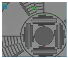
The scale of micromanufactured devices can be difficult to comprehend. Take dust mites. They’re in pillows, bedding, and furniture cushions, but they’re too small to be seen by the human eye. The same is true of the components in a MEMS device. In fact, depending on the device, a MEMS can be smaller than a mite, as shown in figure 1 at right.
The challenges in creating a MEMS device are significant. The manufacturer is wrestling with producing circuitry and components that can’t be seen with the naked eye. Linewidths and other feature sizes are as small as 1/500th the width of a strand of human hair.
MEMS devices are currently being used in inkjet printers, for airbag deployment, as mini-gyroscopes in cars for dynamic stability control, for digital light processing in television sets, and in medical applications. Many laboratory tests are being moved to MEMS devices, for example, disposable blood-pressure tests and blood-sugar analysis for diabetics. In the near future, many common medical tests will be placed on a single MEMS chip.
The metrology challenge for a MEMS or a MOEMS is checking and measuring the circuitry, size, and placement of components to ensure that they fall within specification. Although conventional vision systems may be adequate for measurements in millimeters or even tens of microns, the submicron feature sizes of advanced MEMS and MOEMS packages are typically beyond the capabilities of such equipment. Both FOV and PTP measurements are necessary to ensure quality in MEMS and MOEMS manufacturing.
Many of the advancements in micromanufacturing are the result of processes developed in semiconductor manufacturing. Yield-efficient production of semiconductor devices requires precise alignment between layers, and shrinking circuit geometries on larger wafers have made alignment-related tasks between the layers more challenging than ever. To help with aligning layers, a manufacturer will include a feature called an “overlay” to each layer. Its sole purpose is to compare the location of the overlays to make sure that the alignment of the layers is where it should be. Today, overlay measurements must meet accuracy and repeatability requirements expressed in single-digits of nanometers.
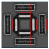 To make accurate and repeatable overlay measurements, vision-based micrometrology systems use image processing in their metrology software to create intensity profiles of the selected overlay pattern in X and Y directions. An intensity profile is a representation of the brightness of each location in the image contained within a specified viewing area. The profile is used to select the features of interest in the overlay pattern. To make accurate and repeatable overlay measurements, vision-based micrometrology systems use image processing in their metrology software to create intensity profiles of the selected overlay pattern in X and Y directions. An intensity profile is a representation of the brightness of each location in the image contained within a specified viewing area. The profile is used to select the features of interest in the overlay pattern.
Any two pairs of features in the intensity profile can be selected as the measurement targets. In most cases, the two sets of targets are the outer and inner geometries of the overlay pattern. Once the system determines the center of symmetry of each pair of targets, it produces overlay measurements by comparing the differences between the locations of the two centers in each direction. This technique minimizes errors due to low contrast, indistinct or irregular edges, and corner rounding.
Semiconductor manufacturers also use automated micrometrology systems to measure the critical dimensions of opaque and transparent areas of chrome photomasks. They measure linewidths; pitch; dimensions of defects, contacts, and corner rounding; optical proximity correction (OPC) patterns; intrusion; extrusions; and other photomask features typically ranging in size from 0.2 µm to 200 µm. Fully automated measurement sequences involve stage positioning, autofocus, image processing, and data output.
 Advanced micrometrology systems offer a number of additional features in their metrology software that improve photomask measurements. Pattern-recognition algorithms accelerate the measurement process by eliminating manual searches for features to be measured. Auto-illumination, which can preprogram the system’s lamps for each measurement, provides the precise illumination control needed to produce consistent image intensity for optimum edge contrast and repeatability. Advanced micrometrology systems offer a number of additional features in their metrology software that improve photomask measurements. Pattern-recognition algorithms accelerate the measurement process by eliminating manual searches for features to be measured. Auto-illumination, which can preprogram the system’s lamps for each measurement, provides the precise illumination control needed to produce consistent image intensity for optimum edge contrast and repeatability.
The most precise systems use proprietary vision-based autofocus algorithms that ensure repeatable focusing of the photomask image by analyzing edge sharpness and contrast through a series of focus positions. For high throughput, laser autofocus can be added to a system.
Although semiconductor-device manufacturing continues to drive accuracy and repeatability requirements of micrometrology systems, the technology is also necessary in producing heads for hard disk drives. To read and write data, a spinning hard disk forces a small amount of air to flow between its surface and the underside of the read-write head. The head is literally floating on a cushion of air. When this airflow has the right volume, pressure, and velocity, the head is correctly positioned relative to the disk surface.
The underside of the disk head has air-bearing surfaces (ABS) and usually includes a series of “steps” that channel the air to create the proper lifting forces. Etched by various means, these steps must be accurate in shape, depth, and location relative to the tip of the read-write magnetic pole. Usually, the required precision is a few tens of nanometers.
To measure critical ABS dimensions, a system must detect the locations of the edges of etched steps that are fractions of a micron deep in a grainy-looking ceramic material. Accurate measurements of these etched steps must be made at high magnifications. The task requires that the system first determine the approximate location of the edge in the FOV image. Automatic pattern recognition helps with this task. The final edge location is determined by collecting data from the image area near the edge. PTP measurements of each of the edges that make up the ABS help determine if the disk head will float as designed. These critical measurements require precise focusing because an edge may be invisible if the focus position is incorrect by as little as 0.02 µm .
Advanced micromanufacturing
methods are constantly being applied to ever-broader ranges of products. The latest vision-based micrometrology systems incorporate cutting-edge positioning technology, high-magnification optics, proprietary application software, high-stability structures, and vibration isolation. In some industries, the systems are making critical one-, two-, and three-dimensional measurements with an accuracy of 10 nm and a repeatability of ± 2 nm. Micrometrology helps manufacturers check the extremely small features of manufactured devices to ensure product quality, prevent costly field failures, and provide the levels of performance that we’ve all come to expect.
Ralph Leseberg, MBA, is managing director at the Micro-Metric division of VIEW Micro-Metrology. He has 10 years experience in metrology plus eight years experience writing software in the semiconductor test arena. Leseberg previously worked at Schlumberger, Advantest, and Sony Electronics.
|
 Real-life applications: MEMS and MOEMS