| by Dirk Dusharme
Semiconductor fabrication is one of the most complex single-part manufacturing processes. From raw silica to packaged integrated circuit (IC), semiconductor fabrication involves more than 200 steps on 75 pieces of equipment, many taking place in a class-one clean room where no more than one particle of dust greater than 0.5 µm is allowed per one cubic foot of air. Yields, the amount of product that passes all tests and makes it into the field, can range from 40 percent for microprocessors to nearly 100 percent for mature, less complex parts. With all of these processes, isolating and reducing variables is a Herculean task--one that is perfect for Six Sigma.
Software Selection
Even with a company as large as National Semiconductor, which has more than 9,000 employees, resources aren’t unlimited. Choosing the right software to meet your needs can make Six Sigma projects run more smoothly and with less wasted time and manpower. During our interviews with National Semiconductor, we noted three software packages that helped CTMG’s Six Sigma projects. These aren’t necessarily the only packages capable of assisting a Six Sigma process, but they are what National Semiconductor considered the best fit for their applications.
Project tracking--Being able to track the progress of multiple Six Sigma projects across multiple sites worldwide would be a huge task without a bit of help. To keep abreast of project status, National Semiconductor utilizes ProjX from Breakthrough Management Group. The software provides CTMG immediate access to project status across all sites with real time dashboards and summary reports. The Web-based application helps centralize project information and make it available to all users via personalized user pages.
Process flow--National uses iGrafx Process for Six Sigma, a process flow and simulation package from iGrafx. With iGrafx, the Six Sigma team is able to simulate existing process flows. Changes can be tested and analyzed for effectiveness before they are actually put in place. Furthermore, data from a simulation can be imported into JMP for data analysis. A visual representation of process flow often leads to a better understanding of the process.
Design of experiments and statistical analysis--The right software can make design of experiments easier and faster by guiding you through the process. National Semiconductor chose JMP statistical software from SAS. The user puts all relevant parameters into the software, including high and low limits for each factor, and then defines the interactions. At the end of each experimental run the user inputs the responses. The software then suggests how to optimize the process.
The value of statistical software with well-designed DOE modules is that it allows users to easily create more complex experiments in a shorter amount of time, allowing the user the ability to explore more interactions.
The fact that JMP integrates with iGrafx Process for Six Sigma is an added plus.
|
Odds are a National Semiconductor IC is within inches of you. It could be in your cell phone, your laptop, your display or any of a dozen electronic devices on your desk or in your briefcase. The Silicon Valley-based chip maker is a leader in analog integrated circuit technology--chips that translate real-world stimuli into digital information.
While National has always prided itself on the quality of its products--its field defective rate is less than 20 defective parts per million--like any company it saw room for improvement, particularly in the area of internal yield. This is why Kamal Aggarwal, executive vice president of National’s Central Technology and Manufacturing Group, mandated last year that all CTMG units would deploy Six Sigma.
“When Aggarwal became executive vice president of CTMG in 1996, his first effort was to improve CTMG’s top metrics: yield, cycle time and cost,” recalls Mark Seay, director of quality and corporate Six Sigma process director. “For the first four to five years that was the focus,” Seay explains. “We made huge progress and got to what would be considered world class in those three areas.”
The next big push came in 2000, with a large CTMG-wide continuous improvement (CI) effort. While the effort yielded good results, it suffered from inconsistency. Each unit--three wafer fabs in Texas, Maine and the United Kingdom; three assembly sites in Singapore, Malaysia and China; and the CTMG headquarters in Santa Clara, California--used its own methods to improve quality. “Everyone was kind of left to their own ways to figure out what [continuous improvement] meant,” recalls Seay. “Certainly there were a lot of improvements made. But it was hard to compare one site to another as far as CI activities were concerned.”
So in 2001, National Semiconductor invited GE Consulting to pitch the Six Sigma concept. The idea met the type of resistance encountered by many companies. All the employees felt that they were “already doing that,” Seay explains. From SPC to FMEA, National Semiconductor process engineers and quality personnel were already using Six Sigma tools and believed that they were “quite good at it,” says Seay. The consensus was that a Six Sigma program would bring nothing new to the table.
Six Sigma was put on the back burner for another year until, at the bi-annual CTMG Summit, Aggarwal brought in another consulting firm to reintroduce Six Sigma. Thomas A. Little Consulting had experience in high-tech processes (disk drive manufacturing) that had a lot in common with semiconductor fabrication and presented a compelling argument for Six Sigma when applied to the semiconductor industry’s highly process-driven manufacturing methods. This was enough to convince C.S. Liu, the senior vice president of National’s plant in Melaka, Malaysia, at the time, to launch a pilot Six Sigma program with 10 projects.
Nine months later at the next CTMG Summit, a key National Semiconductor supplier, DuPont Electronic Technologies, made a presentation on how to quantify Six Sigma. This, coupled with the results of the 10 Melaka pilot projects (initial savings of nearly $900,000 and projected annual savings of nearly $2.3 million) convinced Aggarwal to implement Six Sigma across CTMG. The first wave of projects began in June 2003. Since then, 52 projects have been completed with an 84-percent success rate, resulting in tens of millions of dollars in both hard and soft savings.
In March 2004, CTMG launched its second wave of Six Sigma programs, targeting similar savings from 44 projects. Four of these projects target issues that exist on multiple sites, while nine are aimed at customer satisfaction, quality or safety improvement.
An example of one such wave two project was at National Semiconductor’s South Portland, Maine, facility, which produces advanced CMOS devices for such customers as Samsung, Motorola and Nokia.
The site saw an opportunity to improve yields on a 0.35 µm fabrication process (the smallest feature on the wafers is 0.35 µm) by finding and eliminating sources of variation in the manufacturing flow.
CTMG followed Six Sigma’s DMAIC protocol by taking the following actions. Some of the information is sensitive, so these figures are deliberately fuzzy.
Problem--The fab was experiencing losses at the final electrical test (ET) operation that appeared to be related to excessive current leakage and gate oxide breakdown at the transistors level. A baseline study of this ET yield for an 18-week period at the start of the project showed that there was an opportunity for approximately 1.5 percent additional yield for all wafers in this technology.
Through experience with other technologies, the engineers at National’s South Portland plant knew that their fab was capable of world-class performance for this type of IC, and this yield gap meant that they were leaving more than $1 million in profit on the table.
Goals--Once the team, led by Stephen Swan, senior process engineering manager, and Burcay Gurcan, senior product engineer, had established the yield baseline, the site champion set the goal of eliminating the systematic yield loss caused by transistor leakage and gate oxide breakdown. In addition, the team was challenged with establishing a statistical process control plan for measurement of “critical-to-function parameters” in the process flow that could be used to prevent failing wafers from getting to the final ET step.
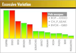
A Pareto chart of the reasons for failed wafers at electrical test identified three process modules that showed excessive variation in the fabrication process. These modules included the spacer formation, channel implants and post-implant acid cleaning steps. Other suspect areas, identified during the team’s brainstorming sessions, were eliminated by performing commonality studies on past events, discussing the issue with industry experts, and re-evaluating experiments that had been previously run.
During the analysis phase, seven factors were determined to have an effect on the three key failure modes. Utilizing the design of experiments (DOE) function of JMP statistical software, the team developed three experiments to determine which interactions had the greatest effect on yield.
 DOE 1--Transistor leakage between drain and source DOE 1--Transistor leakage between drain and source
Failure Modes: Silicon impurities, threshold voltage control, physical damage
Factors: VTN implant, spacer dep, spacer clean, spacer etch
DOE 2--P channel contact leakage
Failure Modes: Fixed charge, silicon impurities
Factors: Post-poly SC1 cleans, HCL:H2O2 clean
DOE 3--Gate breakdown voltage
Failure Modes: Plasma budget, silicon impurities
Factors: Alloy, spacer dep, spacer etch
Prior to running the DOEs, the team had already collected enough information to know that tighter controls were needed on certain in-fab process parameters in the transistor modules. By taking early action to put these controls in place, the team was able to realize some yield improvements after only two months. Once the DOE results came out, the team was able to validate the earlier actions and fully characterize the process window for these critical steps. In the improve step, the team leveraged the results of the DOE’s performed during the previous (analyze) step to make necessary changes to specs, procedures and equipment. These changes ensured that variation during the spacer, implant and acid cleaning steps wouldn’t affect yield at electrical test.
To ensure that the process improvements developed by the team became permanent, a control plan was created and transferred to the manufacturing group. This control plan defined the requirements for every critical-to-function parameter in terms of control charts, control limits, sampling plans, gage capability and out-of-control action plans.
By implementing improved process control methods, the team was able to surpass the initial goal. Moreover, the higher level of performance generated by these process improvements has provided National’s designers with a competitive advantage in their efforts to develop new products for the analog marketplace.
Within six months of starting this project, actions taken increased yield by more than 1.5 percent, with a projected annual savings of $1.1 million. The project lasted about nine months.
CTMG isn’t finished with its Six Sigma journey; wave three was launched at the beginning of this year. The major emphasis will be in design for Six Sigma (DFSS). Pilot programs are underway to enhance the new product phase review system (NPPRS) with DFSS tools/methods in the audio product line. Lessons from that pilot will be used to drive NPPRS improvement across the entire company.
Dirk Dusharme is Quality Digest’s editor in chief.
|

 Measure