| by Thomas Pelton
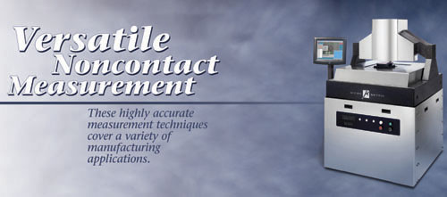
From semiconductor fabrication to hard disk heads, today’s most demanding manufacturing operations require dimensional or positioning accuracies in the micro-inch range. To make the precise measurements needed in these operations, manufacturers often opt for noncontact measuring techniques. With no risk of damage to small, delicate components, noncontact techniques determine the coordinates and critical dimensions essential to ensure product quality.
High-accuracy noncontact measurements can be made by two types of systems: field-of-view (FOV) and point-to-point (PTP). The decision to use one or the other is based on the required accuracy and the size of the area to be measured. When features are so small or so close together that an image of the entire meas-urement distance can be captured within the field of view of a microscope, an FOV system will probably be the more cost-effective choice. PTP measuring systems are more expensive than their FOV counterparts because they include precision positioning components (usually X-Y stages) that allow them to move to various measurement points with the required accuracy.
Precision FOV and PTP systems include several key features that ensure accurate measurements. For example, techniques required to produce nanometer-level precision in FOV measurement applications can be applied to improve PTP measurements. Conversely, robust structure designs and vibration control required to perform precise PTP measurements will also benefit FOV measurements. Such systems achieve the highest precision and repeatability in vision-based measurement of critical dimensions and coordinates. Of primary importance is precise focusing control to ensure that image features are measured under a repeatable focus condition. Sophisticated image analysis with sub-pixel feature detection produces even finer measurements than camera resolution.
For PTP systems, state-of-the-art motion control is essential for accurate position measurements as well as precise positioning of features within the field of view. For positioning accuracy, motion control units include sophisticated servo control with high-precision linear encoders, or laser interferometers for even greater precision.
Precision noncontact measurement systems also require an extremely stable structure that resists vibration and temperature changes, as well as a support platform designed to prevent shock and vibration from degrading measurement accuracy.
In a variety of industry settings, advanced noncontact measurement systems are tackling the toughest applications. Consider the semiconductor fabrication plant, where yield-efficient production requires precise alignment between layers and where shrinking wafer geometries make alignment-related tasks more challenging than ever. Today, overlay measurement must meet accuracy and repeatability requirements expressed in the range of single-digit nanometers.
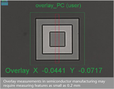
To make highly accurate and repeatable overlay measurements, noncontact systems begin by creating intensity profiles of the selected overlay pattern in X and Y directions. An intensity profile is a representation of the brightness of each location in the image contained within a specified viewing area. The profile is used to select the features of interest in the overlay pattern.
Any two pairs of features in the intensity profile can be selected as the measurement targets. In most cases, the two sets of targets would be the outer and inner geometries of the overlay pattern. Once the system determines the center of symmetry for each pair of targets, it produces overlay measurements by comparing the differences between the locations of the two centers in each direction. This technique minimizes errors due to low contrast, indistinct or irregular edges, and corner rounding.
Semiconductor manufacturers also use automated noncontact systems to measure the critical dimensions of the opaque and clear areas of chrome photomasks. These systems measure line widths, pitch, dimensions of defects, contacts, corner rounding, OPC patterns, intrusion, extrusions and other photomask features ranging in size from 0.2 to 200 µm. They are capable of both manual single measurements and fully automated measurement sequences that involve stage positioning, measurement setup, data processing and output.
Advanced noncontact systems improve photomask measurements with a number of additional features. One is user-friendly pattern recognition software that accelerates the measurement process by eliminating time-consuming searches for items to be measured. Another key feature is auto-illumination, which can be used to pre-program the system’s lamps for each measurement. Auto-illumination provides the precise lamp control needed to produce consistent image brightness for optimum edge contrast and repeatability.
The most precise systems include a proprietary vision-based autofocus that ensures repeatable focusing of the photomask image by analyzing edge sharpness and contrast through a series of focus positions. For high throughput, they also offer a laser autofocus feature.
Micro-electro-mechanical systems (MEMS) are assemblies that combine both electrical and mechanical components on a silicon substrate using microfabrication technology. Their size can range from a few microns to a few millimeters. While MEMS are fabricated using integrated circuit (IC) technology, the process invariably incorporates micromachining, in which selective areas of the silicon wafer are either etched away or built up to form mechanical and electromechanical devices.
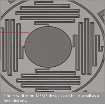
MEMS technology is being used to create actuators and sensors triggered by pressure chemical, fluid, magnetic, thermal, biological and/or motion detection. A typical application is in the automotive industry, where a MEMS or a micro-optical-electro-mechanical system device can sense vehicle attitude and motion for skid prevention and air bag deployment.
The key aspect of MEMS devices is that they incorporate moving components. To do its job, a MEMS device must either cause one of its components to move or allow a component to move based on external influence, and then must sense that motion. The moving component of a MEMS device typically employs a flexure, and the detection of the motion usually involves sets of interleaved “fingers” or “combs.” For precise motion and motion detection, the dimensions of the flexures and motion detection components are very important.
In production, advanced noncontact systems can make highly accurate meas-urements of a variety of critical MEMS dimensions, including the pitch, width, and spacing of flexures, fingers and combs. When utilizing autofocus, the systems provide excellent repeatability when capturing the dimensions of these tiny features.
While wafer geometries continue to drive the accuracy and repeatability requirements of precision noncontact measurement systems, tiny features must also be measured in the production of hard disk heads. Inside a computer, a spinning hard disk forces a small amount of air to flow between its surface and the underside of the read-write head. When this air flow has the right volume, pressure and velocity, the head is correctly positioned relative to the disk surface.
The underside of the disk head is known as the air-bearing surface (or ABS), and usually includes a series of “steps” that channel the air to create the proper lifting force. Etched by various means, these steps must be accurate in shape, depth and location relative to the tip of the read-write magnetic pole. Usually, the required precision is in the range of a few dozen nanometers or less.
To measure ABS dimensions, a system must detect the locations of the edges of etched steps. This is no easy task. The depth of etched cuts can be just a fraction of a micron, making the edges indistinct. Adding to the difficulty is the fact that most heads are made of a grainy-looking ceramic material.
Given the difficulties of edge detection, accurate step meas-urements must be made by a high-magnification noncontact optical coordinate measuring microscope. The task also requires a vision system that can first determine the approximate location of the edge in the image. Once this is done, the system makes the final edge determination by collecting data from the image area near the edge. Besides powerful image-analysis algorithms, suitable systems employ extremely precise focusing because an edge may be invisible if the focus position is incorrect by as little as 0.1 µm.
Advanced noncontact measurement systems incorporate cutting-edge positioning technology, high-magnification optics, proprietary application software, high-stability structures and vibration isolation. In some industries, the systems make critical one-, two- and three-dimensional measurements with accuracy of 10 nm and repeatability of ±2 nm. This measurement prowess helps manufacturers check the extremely small features of manufactured devices to ensure product quality and prevent costly field failures.
Thomas Pelton founded Micro-Metric Inc. in 1979, after noticing a specific need for computer-controlled, noncontact measurement solutions within the semiconductor and other high-technology industries. He has served as president and CEO of the company since its inception. Prior to forming Micro-Metric, he was employed by E. Leitz Wetzlar GmbH, as field service engineering manager for its entire optical product line. He can be reached at tpelton@micro-metric.com.
|